Semiconductor Plasma
Design a Slit HDP Semiconductor Plasma Dry Etcher eBooks & eLearning
Posted by Free butterfly at Aug. 29, 2022
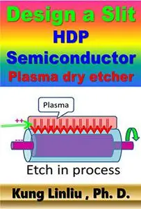
Design a Slit HDP Semiconductor Plasma Dry Etcher by Kung Linliu
English | 2020 | ISBN: N/A | ASIN: B08N1CZHWZ | 83 pages | EPUB | 1.22 Mb
English | 2020 | ISBN: N/A | ASIN: B08N1CZHWZ | 83 pages | EPUB | 1.22 Mb
Design a cylinder HDP semiconductor Plasma dry etcher eBooks & eLearning
Posted by silva1410 at May 21, 2021
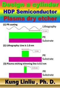
Design a cylinder HDP semiconductor Plasma dry etcher
By Kung Linliu
English | 2020 | ASIN : B08MZXBJ8G | 78 Pages | EPUB | 3.3 MB
By Kung Linliu
English | 2020 | ASIN : B08MZXBJ8G | 78 Pages | EPUB | 3.3 MB
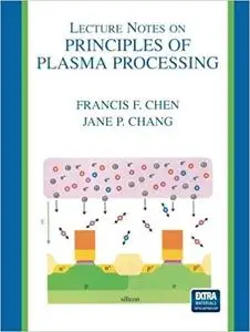
Lecture Notes on Principles of Plasma Processing eBooks & eLearning
Posted by AvaxGenius at March 12, 2024
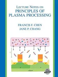
Lecture Notes on Principles of Plasma Processing by Francis F. Chen , Jane P. Chang
English | PDF | 2003 | 213 Pages | ISBN : 0306474972 | 26.1 MB
Plasma processing of semiconductors is an interdisciplinary field requiring knowledge of both plasma physics and chemical engineering. The two authors are experts in each of these fields, and their collaboration results in the merging of these fields with a common terminology. Basic plasma concepts are introduced painlessly to those who have studied undergraduate electromagnetics but have had no previous exposure to plasmas. Unnecessarily detailed derivations are omitted; yet the reader is led to understand in some depth those concepts, such as the structure of sheaths, that are important in the design and operation of plasma processing reactors. Physicists not accustomed to low-temperature plasmas are introduced to chemical kinetics, surface science, and molecular spectroscopy. The material has been condensed to suit a nine-week graduate course, but it is sufficient to bring the reader up to date on current problems such as copper interconnects, low-k and high-k dielectrics, and oxide damage. Students will appreciate the web-style layout with ample color illustrations opposite the text, with ample room for notes.
Nanowires and Nanobelts Materials, Properties and Devices. Volume 1: Metal and Semiconductor Nanowires eBooks & eLearning
Posted by AvaxGenius at March 13, 2024
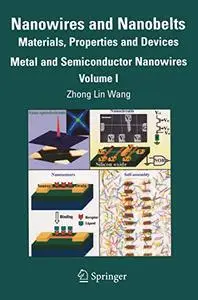
Nanowires and Nanobelts Materials, Properties and Devices. Volume 1: Metal and Semiconductor Nanowires by Zhong Lin Wang
English | PDF | 2003 | 482 Pages | ISBN : 0387287051 | 54.1 MB
Volume 1, Metal and Semiconductor Nanowires covers a wide range of materials systems, from noble metals (such as Au, Ag, Cu), single element semiconductors (such as Si and Ge), compound semiconductors (such as InP, CdS and GaAs as well as heterostructures), nitrides (such as GaN and Si3N4) to carbides (such as SiC). The objective of this volume is to cover the synthesis, properties and device applications of nanowires based on metal and semiconductor materials. The volume starts with a review on novel electronic and optical nanodevices, nanosensors and logic circuits that have been built using individual nanowires as building blocks. Then, the theoretical background for electrical properties and mechanical properties of nanowires is given. The molecular nanowires, their quantized conductance, and metallic nanowires synthesized by chemical technique will be introduced next. Finally, the volume covers the synthesis and properties of semiconductor and nitrides nanowires.
Film Deposition by Plasma Techniques eBooks & eLearning
Posted by AvaxGenius at March 11, 2024
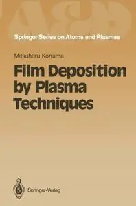
Film Deposition by Plasma Techniques by Mitsuharu Konuma
English | PDF | 1992 | 234 Pages | ISBN : 3642845134 | 28 MB
Properties of thin films depend strongly upon the deposition technique and conditions chosen. In order to achieve the desired film, optimum deposition conditions have to be found by carrying out experiments in a trial-and error fashion with varying parameters. The data obtained on one growth apparatus are often not transferable to another. This is especially true for film deposition processes using a cold plasma because of our poor under standing of the mechanisms. Relatively precise studies have been carried out on the role that physical effects play in film formation such as sputter deposition. However, there are many open questions regarding processes that involve chemical reactions, for example, reactive sputter deposition or plasma enhanced chemical vapor deposition. Much further research is re quired in order to understand the fundamental deposition processes. A sys tematic collection of basic data, some of which may be readily available in other branches of science, for example, reaction cross sections for gases with energetic electrons, is also required. The need for pfasma deposition techniques is felt strongly in industrial applications because these techniques are superior to traditional thin-film deposition techniques in many ways. In fact, plasma deposition techniques have developed rapidly in the semiconductor and electronics industries. Fields of possible application are still expanding. A reliable plasma reactor with an adequate in situ system for monitoring the deposition conditions and film properties must be developed to improve reproducibility and pro ductivity at the industrial level.
Crucial Issues in Semiconductor Materials and Processing Technologies eBooks & eLearning
Posted by AvaxGenius at July 11, 2023

Crucial Issues in Semiconductor Materials and Processing Technologies by S. Coffa, F. Priolo, E. Rimini, J. M. Poate
English | PDF | 1992 | 523 Pages | ISBN : 0792320034 | 60.6 MB
Semiconductors lie at the heart of some of the most important industries and technologies of the twentieth century. The complexity of silicon integrated circuits is increasing considerably because of the continuous dimensional shrinkage to improve efficiency and functionality. This evolution in design rules poses real challenges for the materials scientists and processing engineers. Materials, defects and processing now have to be understood in their totality. World experts discuss, in this volume, the crucial issues facing lithography, ion implication and plasma processing, metallization and insulating layer quality, and crystal growth. Particular emphasis is placed upon silicon, but compound semiconductors and photonic materials are also highlighted. The fundamental concepts of phase stability, interfaces and defects play a key role in understanding these crucial issues. These concepts are reviewed in a crucial fashion.
Plasma processes for semiconductor fabrication eBooks & eLearning
Posted by insetes at Nov. 3, 2020
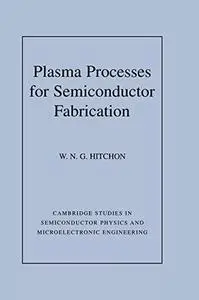
Plasma processes for semiconductor fabrication By W. N. G. Hitchon
1999 | 231 Pages | ISBN: 0521591759 | DJVU | 3 MB
1999 | 231 Pages | ISBN: 0521591759 | DJVU | 3 MB
Plasma Processing of Nanomaterials eBooks & eLearning
Posted by DZ123 at Nov. 4, 2019
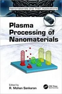
R. Mohan Sankaran, "Plasma Processing of Nanomaterials"
English | 2011 | ISBN: 1439866767 | PDF | pages: 416 | 15.4 mb
English | 2011 | ISBN: 1439866767 | PDF | pages: 416 | 15.4 mb
Plasma Deposition of Amorphous Silicon-Based Materials (Plasma-Materials Interactions) eBooks & eLearning
Posted by insetes at June 21, 2020
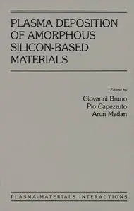
Plasma Deposition of Amorphous Silicon-Based Materials (Plasma-Materials Interactions) By Pio Capezzuto, Arun Madan
1995 | 324 Pages | ISBN: 012137940X | PDF | 18 MB
1995 | 324 Pages | ISBN: 012137940X | PDF | 18 MB
Lecture Notes on Principles of Plasma Processing (Repost) eBooks & eLearning
Posted by step778 at Dec. 18, 2018
Francis F. Chen, "Lecture Notes on Principles of Plasma Processing"
2003 | pages: 248 | ISBN: 0306474972 | DJVU | 6,8 mb
2003 | pages: 248 | ISBN: 0306474972 | DJVU | 6,8 mb